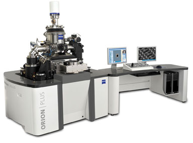
 (Fig.1) Scanning helium ion microscope Zeiss ORION 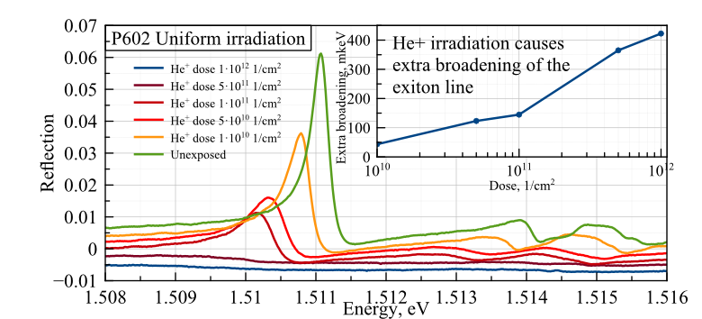 (Fig.3) Extra broadening of the exciton line caused by He+ irradiation 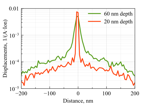 (Fig.5) Lateral displacements in the quantum well 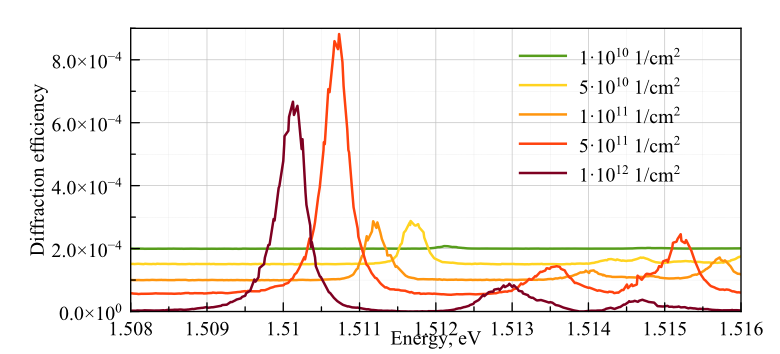 (Fig.7) Diffraction spectra of sample areas exposed with different doses |
The up-to-date Molecular Beam Epitaxy (MBE) technology makes it possible to create quantum-well structures with the exciton resonance width close to its theoretical limit. The forthcoming technical problem lying on the way to the creation of photon logic elements and devices based on these structures is related to searching the method of a controllable lateral fragmentation. Here we present a method of a lateral fragmentation of narrow InGaAs/GaAs quantum wells by a local implantation of He+ ions. We demonstrate a resonant diffraction grating - the structure combining properties of the diffraction grating and spectral selectivity of 2D-exciton resonance. Equipment Lateral fragmentation of the quantum well is performed with a scanning helium ion microscope Zeiss ORION (Fig.1). Focused ion beam penetrates into the sample causing defects in the crystalline framework. These defects result in local inhomogeneous broadening of the exciton line. For the purposes of the sample characterization and induced ion beam effects analysis we use the method of resonant exciton reflection (Fig.2). The optical experiments are performed in Brewster geometry allowing us to dispose of an unnecessary reflection from the sample surface. Detection of reflection spectra is held with a femtosecond laser Spectra Physics Tsunami and МДР-23 spectrometer which has an CCD-line in place of the output slit. Diffraction is detected with tunable CW laser and PMT. Experiment To begin our work we have investigated how the uniform irradiation of ions affects quantum well. On Fig.3 one can see reflection spectra of sample areas exposed with different ion doses and an extra broadening of the exciton line caused by He+ irradiation. Knowing how the ion beam affects optical properties of the quantum well we could make the next step: a diffractional grating. For that purpose we have exposed a periodical pattern on the sample with a He+ beam: 375 uniformly irradiated stripes 150mkm in height and with a period of 800nm (Fig.4). Ion doses used in our experiments are several orders less than those needed for etching process to begin. So the only difference between irradiated and unexposed areas lies in the quality of the quantum well. Dark grey stripes corresponds to irradiated areas of the sample, while the light grey - to unexposed areas. The modelling process of an ion scattering using the Monte-Carlo method gives us the distribution of the number of induced defects inside the crystallic structure depending on the distance from the middle of an ion beam for the certain depth of location of quantum well (Fig.5). This distribution consists of 2 gauss curves - one narrow intence (initial beam defects) and wide (secondary beam). Distant slopes of the wide gauss curve significantly decrease the quality of the quantum well in light stripes of the grating. Illuminating ion patterned areas of the sample with the monochromatic laser light with a wevelength adjusted right into an excitonic resonance another canalised coherent signal appears (Fig. 7). This signal demonstrates clear resonant properties and travels in the direction corresponding to the 1st diffractive order of an 800nm grating enlightened at 74 degrees (Brewster angle for GaAs). Discussion In this work we've shown the possibility of making Diffractive Optical Elements locally changing optical properties of the quantum well with low intensity He+ ion beam. The demonstrated resolution is smaller than 800 nm. The most important task is to achieve spatial resolution of fragmentation sufficient for lateral quantization of excitons in quantum wells. For the III-V single quantum well structures, the needed size of the fragment is 40-50 nm. This work was performed on the equipment of the SPbU Resource Centers 'Nanophotonics' and 'Nanotechnology'. The reported study was supported by RFBR, research project N. 14-02-31617 mol a. |
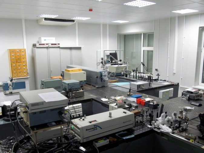 (Fig.2) Optical setup for sample characterization 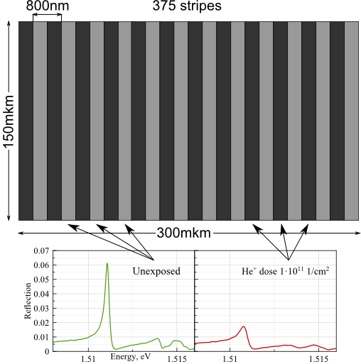 (Fig.4) Diffraction grating 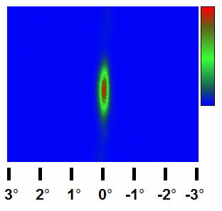 (Fig.6) Diffraction signal detected by a CCD array |

 English
  Русский