Creation and characterization of DBR/TIR waveguides

Exciton-Polaritons in Planar Total Internal Reflection Waveguides

Since the discovery of the strong coupling between an electromagnetic field and material resonances there is a constantly raising interest in exciton-polariton investigations in semiconductor heterostructures. These quaziparticles, originating from the photon-exciton interaction, inherit designatory properties from both parents: a strong nonlinearity through the exciton-exciton interaction and small effective mass from the photonic part. Researchers worldwide have succeeded in observing a number of important quantum effects on exciton-polaritons in high finesse DBR microcavities with quantum well: stimulated polariton scattering, Bose-Einstein polariton condensation and polariton condensate superfluidity.

In the last years significant steps have been made in using planar waveguides as a media for observing propagating polaritons with large propagation distance values. Planar total internal reflection (TIR) waveguides have several essential advantages over those based on DBR microcavities: relatively small heterostructure thickness, growth construction simplicity and almost complete absence of light leakage from the waveguide. These factors and a perfection of molecular beam epitaxy technology for QW production give grounds for high expectations in observing a strong coupling effect in such systems.

Experiment

Here we explain experimental approach and present results obtained for sample T699p2: an asymmetrical TIR-waveguide with 930 nm thick Al3%GaAs core and 13.7 nm GaAs quantum well in its midpoint. A vacuum and 960 nm thick Al30%GaAs serve as cladding layers.

First we need to solve a problem of injecting the light inside the sample. It is impossible to directly excite the TIR-waveguide from the upper or lower half-space, because you can't achieve light propagation angles exceeding the characteristic angle for cladding-core surface. The obvious solution lies in enlighting the sample from the sidewall. But because of near-wavelength thickness of the core layer (930 nm) this choice requires solution of several complicated engineering challenges: microlens placement inside the cryostat cold head, a perfect optics adjustment and a complete absence of any vibrations in the scheme.

Turns out that light injection in the TIR-waveguide core can also be performed through a grating coupler placed on the sample surface. It allows to bypass the Snell refraction law and with a careful choice of parameters to obtain any desired light propagation angle in the core. With a technology of Ar+ ion etching though an electron-beam lithographed PMMA mask a set of square 300 mkm wide diffraction gratings with a period of 250 nm and 100 nm depth was planted on the sample surface. The period was chosen to allow the existence of only 1 diffraction order inside the waveguide core with the diffraction angle of ~70°, what is almost equal to the lowest index mode of the TIR-waveguide with given layer composition. The results presented here were obtained for the grating #3 with the 100 mkm distance from the end of the grating to the cleaved edge of the sample (Fig.1).

During the measurement process the sample was kept in closed cycle helium cryostation Cryomech ST15 at the temperature 10K. The light of CW tunable Sacher Lasertechnik Lynx TEC-120 laser was injected into the lowest index mode of the TIR waveguide by the first diffraction reflex of the grating. We collect the light outcoming from the waveguide edge in a wide spatial angle with a short-focus lens and detect if with a PMT (Fig.2). The experimental setup allows us to perform fast scanning of an incidence angle α and slow scanning of laser light energy E.

Results

Away from exciton resonances this intensity-angle dependence for a single wavelength value has a maximum corresponding to the photon mode in TIR-waveguide with polarization splitting of around 4 meV. At the energies close to the resonances of exciton with heavy hole (HH) and light hole (LH) we observe an anticrossing effect due to the strong coupling between photon and exciton modes (Fig.3&4). A maximum splitting for HH-exciton was observed in S polarization (with the Rabi splitting ΩHH, S = 2.6 meV). For LH-exciton – in P polarization with ΩLH, P = 2.8 meV.

The reported study is partially supported by RFBR, research project No. 15-02-07668 a.
This work is carried out on the equipment of the SPbU Resource Center “Nanophotonics” (http://www.photon.spbu.ru).

For more information on exciton-polaritons in planar waveguides and DBR-microcavities check the following publications:
[1] C. Weisbuch, M. Nishioka, A. Ishikawa, and Y. Arakawa, Phys. Rev. Lett. 69 N23, 3314 (1992).
[2] J. Kasprzak et al., Nature 443, 409-414 (2006).
[3] A. Amo et al., Nature Physics 5, 805-810 (2009).
[4] P. M. Walker et al., Appl. Phys. Lett. 102, 012109 (2013).

For more information on quantum wells and advances of MBE-technology check the following publications:
[1] S.V. Poltavtsev et al., Solid State Comm. 199, 47-51 (2014).
[2] I.A. Solovev et al., Journal of Physics: Conference Series 643, 012085 1-4 (2015).

Download PDF


Fig.1. Diffraction grating etched on the sample surface by Ar+ ions through an electron-beam lithographed PMMA mask.


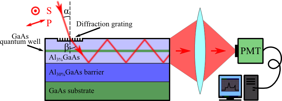
Fig.2. Scheme of the experiment.


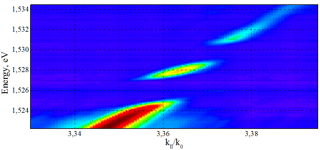
Fig.3. Three-dimensional data obtained in the experiment: energy-angle dependence of the signal intensity.


Fig.4. Angle-resolved spectral positions of signal maxima and spectral dependence of the peak intensity.

Lateral fragmentation

Scanning helium ion microscope Zeiss ORION
(Fig.1) Scanning helium ion microscope Zeiss ORION

Extra broadening of the exciton line caused by He+ irradiation
(Fig.3) Extra broadening of the exciton line caused by He+ irradiation

Lateral displacements in the quantum well
(Fig.5) Lateral displacements in the quantum well

Diffraction signal
(Fig.7) Diffraction spectra of sample areas exposed with different doses

The up-to-date Molecular Beam Epitaxy (MBE) technology makes it possible to create quantum-well structures with the exciton resonance width close to its theoretical limit. The forthcoming technical problem lying on the way to the creation of photon logic elements and devices based on these structures is related to searching the method of a controllable lateral fragmentation.

Here we present a method of a lateral fragmentation of narrow InGaAs/GaAs quantum wells by a local implantation of He+ ions. We demonstrate a resonant diffraction grating - the structure combining properties of the diffraction grating and spectral selectivity of 2D-exciton resonance.

Equipment

Lateral fragmentation of the quantum well is performed with a scanning helium ion microscope Zeiss ORION (Fig.1). Focused ion beam penetrates into the sample causing defects in the crystalline framework. These defects result in local inhomogeneous broadening of the exciton line.

For the purposes of the sample characterization and induced ion beam effects analysis we use the method of resonant exciton reflection (Fig.2). The optical experiments are performed in Brewster geometry allowing us to dispose of an unnecessary reflection from the sample surface. Detection of reflection spectra is held with a femtosecond laser Spectra Physics Tsunami and МДР-23 spectrometer which has an CCD-line in place of the output slit. Diffraction is detected with tunable CW laser and PMT.

Experiment

To begin our work we have investigated how the uniform irradiation of ions affects quantum well. On Fig.3 one can see reflection spectra of sample areas exposed with different ion doses and an extra broadening of the exciton line caused by He+ irradiation.

Knowing how the ion beam affects optical properties of the quantum well we could make the next step: a diffractional grating. For that purpose we have exposed a periodical pattern on the sample with a He+ beam: 375 uniformly irradiated stripes 150mkm in height and with a period of 800nm (Fig.4). Ion doses used in our experiments are several orders less than those needed for etching process to begin. So the only difference between irradiated and unexposed areas lies in the quality of the quantum well.

Dark grey stripes corresponds to irradiated areas of the sample, while the light grey - to unexposed areas. The modelling process of an ion scattering using the Monte-Carlo method gives us the distribution of the number of induced defects inside the crystallic structure depending on the distance from the middle of an ion beam for the certain depth of location of quantum well (Fig.5). This distribution consists of 2 gauss curves - one narrow intence (initial beam defects) and wide (secondary beam). Distant slopes of the wide gauss curve significantly decrease the quality of the quantum well in light stripes of the grating.

Illuminating ion patterned areas of the sample with the monochromatic laser light with a wevelength adjusted right into an excitonic resonance another canalised coherent signal appears (Fig. 7). This signal demonstrates clear resonant properties and travels in the direction corresponding to the 1st diffractive order of an 800nm grating enlightened at 74 degrees (Brewster angle for GaAs).
We exposed 5 gratings with different ion doses. A spectral dependence of signal in the diffraction channel of the detection scheme is shown on Fig.6.

Discussion

In this work we've shown the possibility of making Diffractive Optical Elements locally changing optical properties of the quantum well with low intensity He+ ion beam. The demonstrated resolution is smaller than 800 nm. The most important task is to achieve spatial resolution of fragmentation sufficient for lateral quantization of excitons in quantum wells. For the III-V single quantum well structures, the needed size of the fragment is 40-50 nm.

This work was performed on the equipment of the SPbU Resource Centers 'Nanophotonics' and 'Nanotechnology'. The reported study was supported by RFBR, research project N. 14-02-31617 mol a.
http://www.photon.spbu.ru, http://www.nano.spbu.ru

Femtosecond laser Spectra Physics Tsunami
(Fig.2) Optical setup for sample characterization

Diffraction grating
(Fig.4) Diffraction grating

Diffraction signal
(Fig.6) Diffraction signal detected by a CCD array